Many applications require equipment to be in service for several decades following the initial delivery. This might include supporting the equipment in the field or the expectation of new systems being available for order over several years. This is often the case in the military and aerospace environments, where projects have lifespans of 20-plus years.
ASIC nodes have shrunk dramatically, and older technologies have become obsolete due to the end of foundry support. This is caused by demand or economic issues, the obsolescence of materials, or the tools or equipment being phased out. Procurement can help to a limited degree with ‘last-time’ buys of ASICs. However, to ensure future deliveries, it is often required to undertake a more structured obsolescence management approach and migrate the legacy ASIC or FPGA design to a newer FPGA device.
If you are inheriting a legacy FPGA design, while the device will probably still be available, it is often necessary to make design revisions and changes to the legacy design to support system-level obsolescence (e.g., ADC or DAC components becoming obsolete, requiring new ones to be designed in).
Of course, to successfully migrate a legacy ASIC or FPGA, you need to thoroughly understand the design. Sadly, often over the years, design documentation has been misplaced or lost, while the engineering team may have moved on or retired.
The key to being able to perform a successful migration or update is understanding the legacy design in-depth. Having a detailed understanding of the design enables optimal decision-making.
Key aspects that need to be understood are:
- Functionality – What is the functionality of the design, how do the submodules function?
- Hierarchy – What is the hierarchy of the design?
- Clocks and Clocking Structures – What are the clocking structures used in the design? Are there any instances of clock gating or clock domain crossings, etc.?
- Reset and Reset Structures – What is the reset structure used throughout the design?
Blue Pearl’s Visual Verification Suite (VVS) has several features that can be used when working with legacy designs to help the designer understand and migrate the design successfully.
Schematic
Loading the original RTL into VVS will result in a schematic that can be viewed and explored. Unlike vendor implementation tools, no synthesis is required, so the schematic view is made available in seconds. Once loaded, the engineering team can navigate the schematic and determine the construction of the design.
The schematic view has several perspectives available:
- Full Schematic – Full schematic
- Block Schematic – Showing the functional blocks and interconnects
- Clock and Reset – Showing Clock and Reset connections to blocks
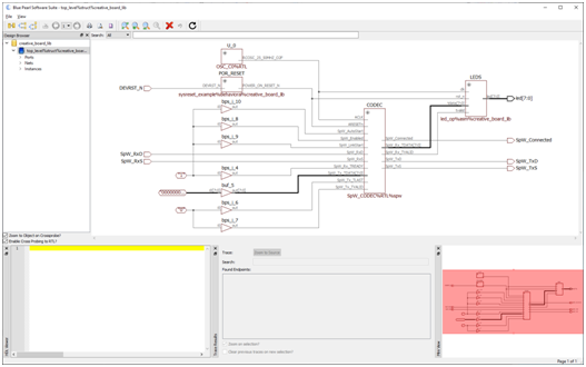

Within the schematic, cross-probing is possible between the schematic and RTL elements to help gather further information on the design’s operation.
FSM Viewer
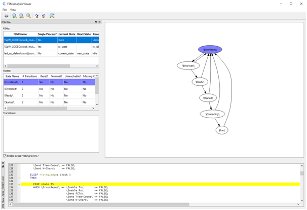
While the schematic viewer is excellent for enabling developers to understand the architecture of the design, the FSM viewer enables developers to view the state diagram for each Finite State Machine (FSM) within the design. Just as with the schematic viewer, each state machine, transaction, and state can be cross-probed with the RTL, enabling a deeper understanding of the particular FSM.
Static Analysis Checks
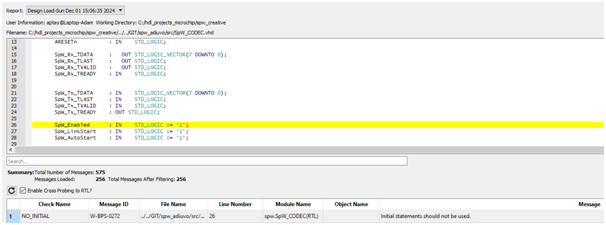
Coding styles change between ASICs and FPGAs. Legacy FPGA designs may have been functioning in the field for years but still contain latent issues that remain unresolved. This is where VVS’s static analysis checks become very important.
With over 400 static analysis checks ranging from FSM styles to compliance with industry best practice coding standards like DO-254, these checks are applied as the design is loaded. They provide the developer with a list of violations that can be investigated as part of the design migration or update.
Clock Domain Crossing
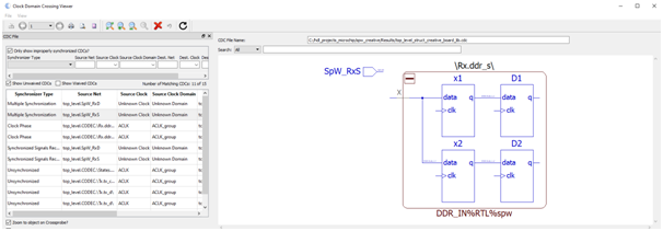
Migrating a design requires understanding the clock domains within the design. Within VVS, the Advanced Clock Environment can be used to help analyze the clock domains and generate the SDC constraints.
To ensure safe clock domain crossings in the migrated design, CDC analysis can be used within VVS to identify and address unsafe crossings. If there are any unsafe clock domain crossings, these can be visualized and cross-probed to the source RTL for corrective actions.
Path Analysis
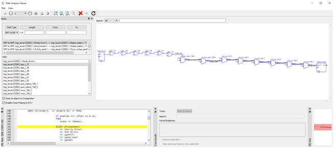
The ultimate goal of design migration or legacy design updates is to achieve timing closure in the new device. One aspect that might change as the design is updated or migrated is the longest path within the design. This path may have been acceptable in the previous technology but could now cause issues.
With VVS, once the design has been updated, and prior to synthesis and implementation, the developer can run the path analysis. This analysis quickly identifies the longest path within the design (e.g., between registers, input to output, or input to register/register to output).
This enables the developer to enter synthesis and implementation with higher-quality code.
Conclusion
The capabilities provided by Blue Pearl’s VVS enable FPGA developers to understand and effectively work with legacy ASIC and FPGA designs that need migration or updating to address obsolescence. Every company that needs to update legacy designs should have VVS in their toolbox.
About Blue Pearl Software
Blue Pearl Software, Inc. is a leading provider of DO-254 compatible design automation software for ASIC, FPGA and IP RTL verification. Our customers are RTL managers and developers in military, aerospace, semiconductor, medical, communications and safety critical design companies. The Visual Verification™ Suite speeds block and project level verification with advanced integrated RTL structural and formal linting, constraint generation and clock domain crossing analysis. Our usability is unmatched in the industry and can help your design team accelerate development and produce high reliability designs.
To learn more about the Visual Verification Suite, please request a demonstration.