FPGA designs are increasingly used for high reliability applications such as aerospace, medical, industrial, and automotive. Failure of the FPGA design in these applications could lead to injury, loss of life or environmental disaster. It is therefore critical that the design behaves as we intend and not as the synthesis or implementation tool thinks it should.
Of course, FPGA designs are sequential in natures and use counters, state machines and shift registers etc. to implement the functionality required. However, to control the next state logic or next counter increment we naturally use combinatorial logic.
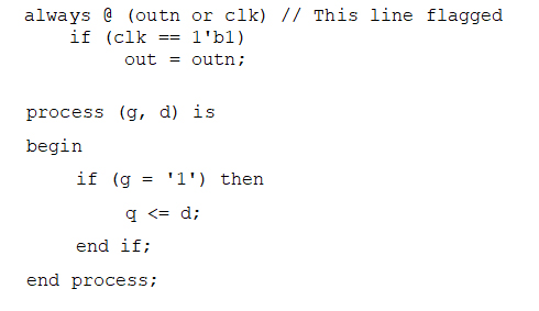
The behaviour of the combinatorial logic is described in processes (VHDL) or always blocks (Verilog). The output(s) of the combinatorial block should be a function of the inputs only and not previous inputs. If we fail to fully describe every possible input condition, the synthesis tool will need to implement memory for those missed input states. To implement this memory the synthesis tool will insert a latch, often referred to as an implied latch.
Typical Coding structures which will create latches in Verilog and VHDL are shown below. Note how the combinatorial logic is incomplete.
When designing for high reliability applications, failure to fully define the output for a set of given input conditions can result in a significant design issue. As such, the implementation of an inadvertent latch in your design is something which should be detected and corrected.
Failure to fully define the behaviour of a combinatorial circuit may lead to unexpected behaviour and differences between synthesis and simulation. Functionally, as latches are enabled potentially for a longer period than synchronous flip flops are, in high reliability designs this increases the possibility of a Single Event Transient being captured and stored in the latch, further impacting the circuit behaviour.
This can have a significant impact on the probability that a SET will be captured at the end point when analysed compared to a combinatorial path and synchronous design.
However, even if your application is not high reliability, we need to consider the other impacts using a latch might have on your design.
Timing and placement may become an issue – for example Xilinx UltraScale CLB contains 16 storage elements (2 per LUT). Within a CLB these 8 LUT and 16 Storage elements are split top (A-D) and bottom (E-H). Each element top or bottom can be defined as either register or latch – thus selecting one latch means the remaining 7 must be latches or unused. This can influence the timing of the design due to placement of the latch resource in relation to the registered elements as the routing path is increased. This can lead to issues achieving timing closure.
In addition, latches may also result in a situation which reduces the ability of the timing engine to accurately determine the timing relationship where latches are involved. The timing engine is developed to accurately close timing when synchronous design is used. As such, timing paths may be incorrectly analysed and optimised where latches are involved. This could lead to the inclusion of latent issues yet to arise.
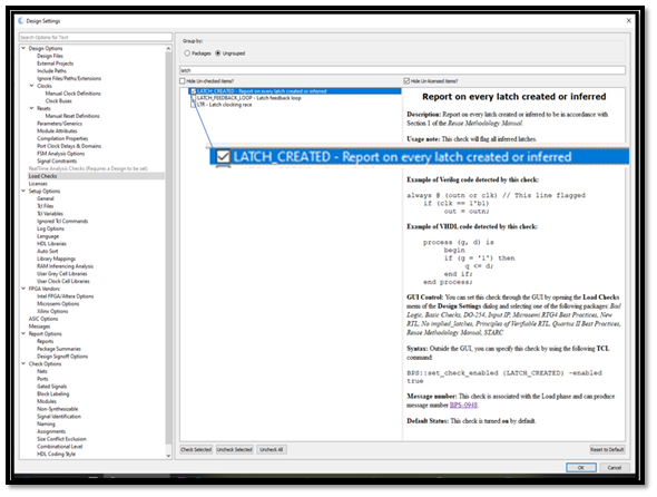
Being able to find inadvertent latch creation early in the design process is critical to entering simulation and synthesis with a better quality of code. This is where Blue Pearl can assist developers, using its structural RTL analysis to quickly identify latches in both Verilog and VHDL.Enabling the LATCH_CREATED check (one of the 300+ structural coding checks available during the load phase) will identify any latches within the design.
Once identified they can be quickly corrected prior to running simulation and then synthesis. Of course, synthesis will report latches have been created in the synthesis report; however, by this time the verification may have been completed. Re-running verification to ensure the behaviour is the same once the latches have been created will be time consuming and costly.