Category Archives: Blog

Issue 6: BPS Integration with Vivado and Vivado HLS

Modern FPGA designs are complex systems. They may include processor cores, RTL code and, increasingly, modules developed using High Level Synthesis (HLS).

Of course, we still want to analyse the custom RTL created and the overall design for compliance with design methodologies e.g. STARC, Reuse Methodology Manual and Xilinx UltraFast Design Methodologies. We may also want to analyse at the design level to ensure all Clock Domain Crossings (CDC) are safe, along with identifying Longest paths and False and Multi Cycle paths which will impact timing constraint creation.

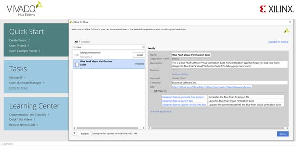
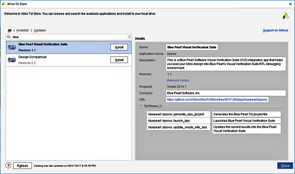
When we are working with Xilinx devices, we can include the Blue Pearl TCL Store Add Ins. These enable us to create new projects, as well as load and update a design from Vivado directly into BPS.

vivado_1

Figure 1 – Blue Pearl TCL Store Add in

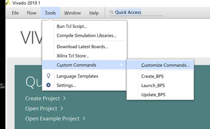
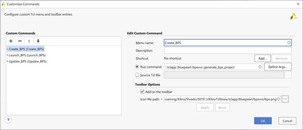
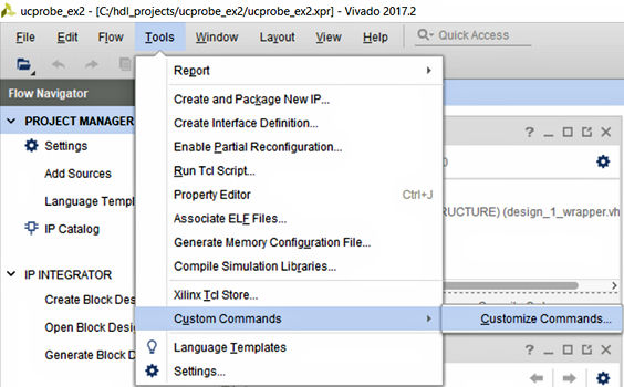
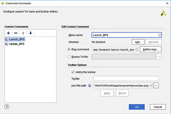
Once the BPS scripts have been installed, we can use the Tools menu to create three new custom commands: Create_BPS, Launch_BPS and Update_BPS.

vivado_2

Figure 2 – Defining the Custom Commands

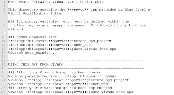
We can find each of the TCL commands to be used for each custom command in the readme file installed with the TCL store add in. On my windows system this was available under the following location.

C:\<user>AppData\Roaming\Xilinx\Vivado\2019.1\XilinxTclStore\tclapp\bluepearl\bpsvvs

vivado_3

Figure 3 – Readme file with commands for Vivado Integration

You can also find a logo under the same directory that can be used to label the commands.
vivado_4

Figure 4 – Setting the BPS Commands

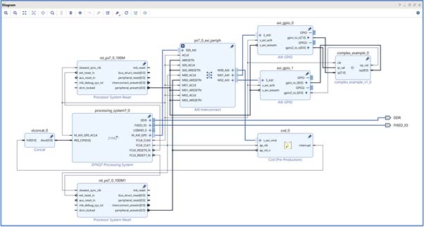
With the TCL store integrated we can then create our design. I used the following to demonstrate a design of sufficient complexity:

  • Zynq Processing System Configured for ZedBoard
  • HLS Callendar Van Dusen Equation – This design uses floating point representation.
  • RTL Implementation of the Callandar Van Dusen Equation – This design uses IEEE VHDL 2008 Fixed Point number representation.
  • AXI Interconnect – Connects the HLS and RTL blocks to the processor enabling a SW based solution.
  • Processor Reset Blocks

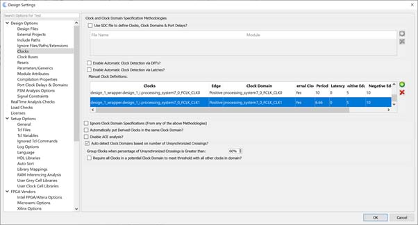
To create a sufficiently complex clocking scheme, the HLS and RTL blocks will be placed on different clock domains (FCLK0 and FCLK1).

The complete design looks as below.
vivado_5

Figure 5 – Vivado Design

Once the design has been completed in Vivado, we can generate the output products and use the Blue Pearl TCL store commands to create a new project, and then open the project in BPS.

This will contain all of the RTL files used within the design and represent not only the custom developed RTL but also the RTL created IP blocks and the HLS block.

Before we can get the design to successfully load for analysis, we need to make some changes to the design settings. This includes:

  • Setting the VHDL Language 2008 – this is due to the use of the fixed-point libraries in the RTL module
  • Set the Xilinx Libraries to the correct version – In this example I used Vivado 2019.1

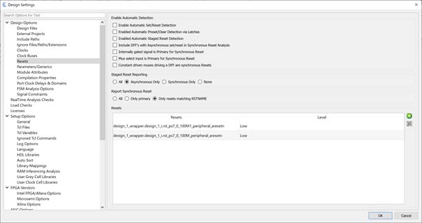
I also defined the Clocks and the Reset from the Processing block. These are defined in the Design Settings -> Clocks and Design Settings -> Reset tab

vivado_6

Figure 6 – Setting the clocks

vivado_7

Figure 7 – Setting the design Resets

With these changes we can then successfully load in the design to BPS and start analysing and filtering the load messages.

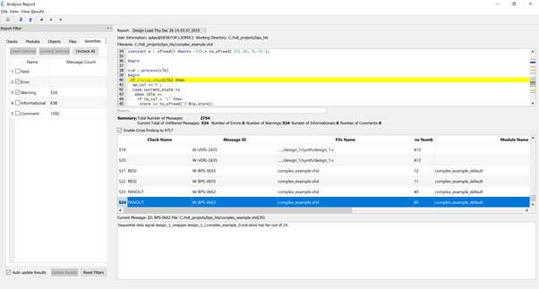
By opening the results view and looking through the detailed messages, we can then assign waivers to the messages raised. These waivers indicate if the message needs to be addressed (Must Fix) or does not need to be fixed (Won’t Fix).

When we are working with large groups of messages, we can use regular expressions to waive several messages to either must or won’t fix at once, easing the analysis.

Once this analysis is completed, we will have several issues remaining in the design which are flagged as Must Fix.

vivado_8

Figure 8 – Report Viewer

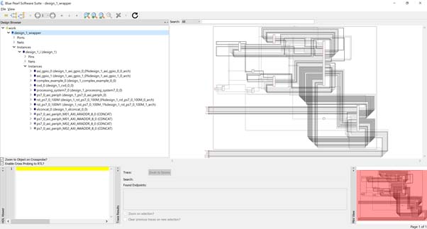
We can also observe the design in the schematic viewer to ensure the design architecture looks like the block diagram in Vivado.

vivado_9

Figure 9 -Top Level Schematic

Within the schematic view we can double check to see that all the instances included in the Vivado design are visible.

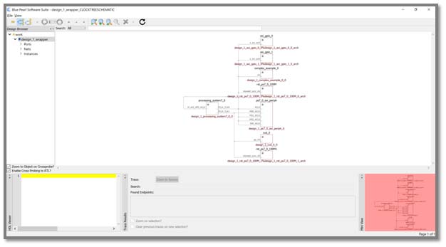
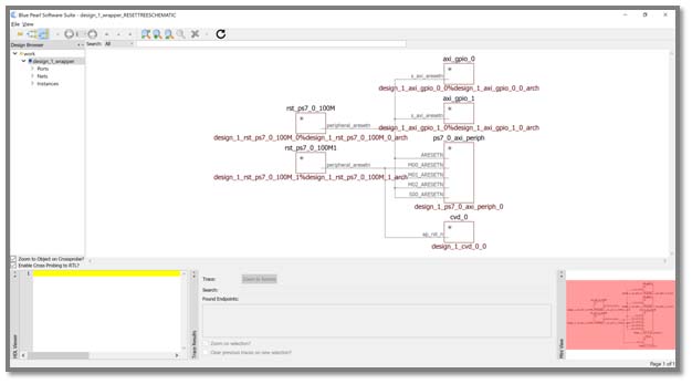
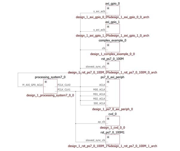
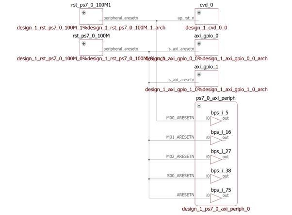
We can also configure the schematic viewer to observe the clock and reset trees within the design using the Clock Tree Schematic and Reset Tree Schematic views.
vivado_10

Figure 10 – Clock Tree Schematic Diagram

vivado_11

Figure 11 – Reset Tree Schematic View

With the design loaded we are then free to explore the FSM viewer to analyse any issues raised in the load analysis.

vivado_12

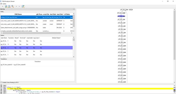
Figure 12 -FSM Analysis listing of all FSM within the design

All this information is available as soon as the design loads. We can also then run design analysis to identify any issues such as clock domain crossing, path analysis and false / multicycle paths.

vivado_13

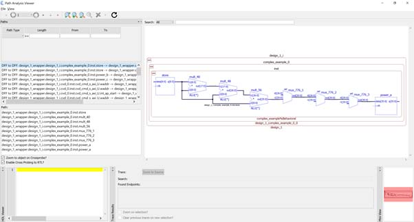
Figure 13 – Path Analysis

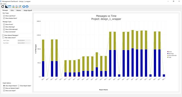
Finally, you can observe the maturity of the design as it passes through the load and analysis phases using management dashboard. This enables us to see the number of open issues and therefore the project maturity we progress through the design cycle.

vivado_14

Figure 14 – Management Dashboard

Wrapping up, we can see that we have been able to load in a complex design which consists of different elements e.g. processing system, HLS IP and Standard Xilinx IP into Blue Pearl Software and this enables us to check for design level issues.

You can find the example Blue Pearl and Vivado projects here.

Issue 5: State Machine Design & Analysis

State machines are at the heart of our designs. They enable us to implement sequential structures in a parallel programmable logic world. We use them to implement control structures and communication protocols, however complex state machines design can also significantly slow down our development due to the challenges associated in debugging issues, epically if only using simulation for verification.
Let’s look at some simple steps we can take when implementing state machines to reduce the number of potential issues introduced, along with how to analyze them using Blue Pearl’s Visual Verification™ Suite to accelerate debug before simulation.

When developing a state machine, it is good practice to ensure our design uses the following factors:

  • Implement all the functionality in a single clocked process. This prevents the implementation of latches or un-synthesizable combinatorial logic constructs. It also ensures all outputs from the state machine are clocked. A single process state machine also prevents mixed decoding of the present and next state in the design, as there is only one state. Single process state machines are also easier to debug if necessary.
  • Ensure the state machine has a clearly defined reset state. When defining this state, do not rely on positional association of the reset state in the state definition.
  • Decouple as much functionality as possible from the state machines. Do not decode large buses or counters within the state machine body. In place of this, pass single bit inputs and outputs from the state machine to start counters or indicate that the counter has reached its terminal value. This decouples large elements of logic from the state machine implementation, allowing for a better implementation and improved timing.
  • If the state machine does not use a power-of-two states and the application is a high reliability or mission critical implementation, ensure that the unused states are correctly addressed so the state machine does not lock up if an unused state is entered due to noise or single event effects. Correctly addressing unused states means ensuring that for each unused state there is a recovery to a known state so operation can continue.

Once we have implemented our state machine design, the next stage is to integrate it within the larger design and then analyze the design using Visual Verification Suite.

Analyzing our state machines in Visual Verification Suite is very simple and performed as part of the load process. Before we load our design and perform the FSM analysis, we need to first configure the analysis.

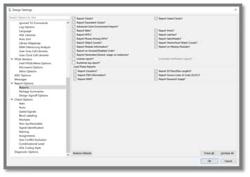
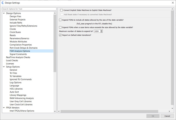
The first step is to define the FSM Analysis options. Here we can configure what analysis is performed. One of the crucial options is the conversion of implicit state machines to explicit state machines; without this an implicit state machine may not synthesize.

If you are not familiar with implicit state machines, they are the state machines which are defined in a more traditionally software style consisting of loop, branches and wait states.

design-settings

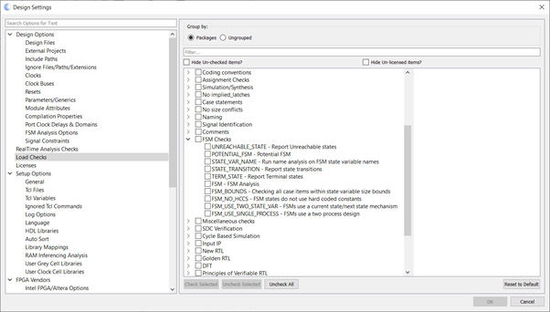
Once the FSM analysis is correctly configured, we can define further checks on the FSM under Load Checks. Here we can define which rules we wish to use to check our state machine, such as checking that the state machine is implemented using a single or two process structure as required by our design rules (FSM_USE_SINGLE_PROCESS and FSM_USE_TWO_STATE_VAR).

We are also able to check to ensure there are no unreachable states or terminal states included within the design. For safety critical / high reliability applications, the ability to ensure that unused states are correctly addressed in the design is very important, since once entered they become terminal states if not correctly addressed.

Terminal states can occur if unused state states are incorrectly addressed, or due to design error where a state is entered but the logic to exit that state is not implemented correctly.

With the options configured in line with the design standards, the design settings window can be closed and the design loaded, which runs the analysis.

design-settings2

Once the design is loaded, we can view the FSM analysis results. These are available in both as messages in the results view, and graphically in the FSM Analysis View.

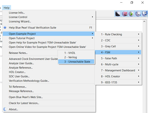
To demonstrate the capabilities of the FSM analysis we will use the unmapped state example, which can be found under the help menu.

help

This will load in an example Verilog file which contains a state machine which has a design issue.

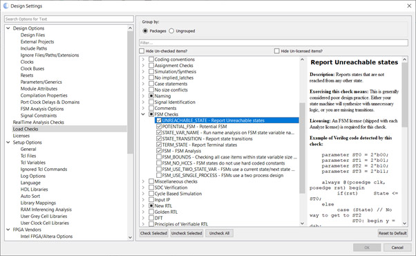
Before the design is loaded and analyzed, click on the design settings to see how the FSM analysis for this example is configured.

design-settings3

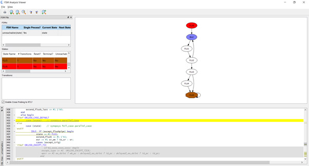
Loading the design will perform the FSM Analysis, and results will be available under the “View Results” option and the FSM Analysis Viewer.

fsm-analysis

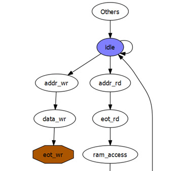
Looking at the FSM Analysis Viewer we will notice that this design has a terminal state for state five, which results in state six being unreachable. Both have colors (brown and red respectively) to show the states where issues exist.

Having identified this issue in the FSM Analysis Viewer we are then able to correct the RTL source to behave as intended.

This ability to enforce good design practice and analyze the FSM behavior quickly enables us to identify issues earlier in the RTL source code, which can save time in development process as issues are identified before simulation and synthesis.

Issue 4: Creating our own Packages

One of the reasons we use Blue Pearl’s Visual Verification™ Suite is to enter simulation and synthesis with a better quality of code. Improved code quality means we have identified and addressed coding standard violations, structural logic issues, long combinatorial paths and of course, clock domain crossing issues.

To ensure the same quality across several modules and projects we need to ensure each project and module is subject to the same design checks. This is where creating a “custom package” comes in very handy.

Within a custom package we can group together all the relevant design checks and then use the package each time Analyze RTL™ or CDC is run. Typically, we will base the custom package on our own development rules and guidelines, also known as coding standards.

Let’s look at how we can create and use a custom package using Blue Pearl Software Tcl commands. The Tcl script will be loaded when Visual Verification Suite starts, configuring the packages and checks we desire to be run.

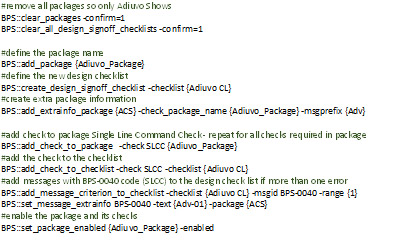
Creating a script is easy and can be achieved in just a few lines of code as you can see in the completed code snippet below.

The Tcl script will initially clear all the existing packages and design signoff checklists such that the only package which appears in the Design Checks window is the one we are going to create in a few lines time. To do this we use the Tcl commands BPS::clear_packages and BPS::clear_all_design_signoff_checklists.

The second step is to define the new package and design signoff checklist, though to run the design signoff checklist a Management Dashboard license is required. In this case I am creating a package called Adiuvo Package using the Tcl commands BPS::add_package {Adiuvo Package} and a check list called Adiuvo CL with the command BPS::create_design_signoff_checklist -checklist {Adiuvo CL}.

Once the new package and checklist have been declared we can enable the design checks, while also adding these checks to the newly created checklist. In this example, for simplicity the package contains only a single check so there is only a single command on each line.

The completed Tcl is shown below:

1_first

Tcl Script

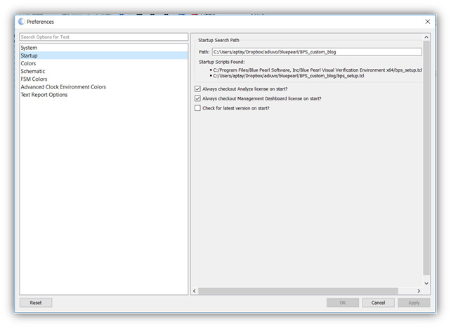
To use the Tcl script that we have just created, we need to rename it to bps_setup.tcl, and set the startup search path to include the directory where our bps_setup.tcl script is contained.

We set the startup search path in the preferences, once we set this to our Tcl file, we can restart.

2_tclfile

When suite restarts up, you will see in the message window the new Tcl script being loaded.

3_suiterestartup

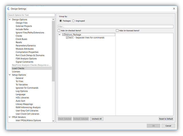
Once it has finished loading, if we open the design settings window, viewing the load checks will show the Adiuvo Package and the check which was enabled as part of it.

4_designsettings

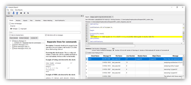
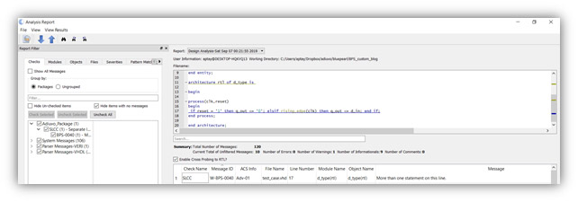
Running this check package against, a test case will result in the warning below being issued, as you would expect.

5_report

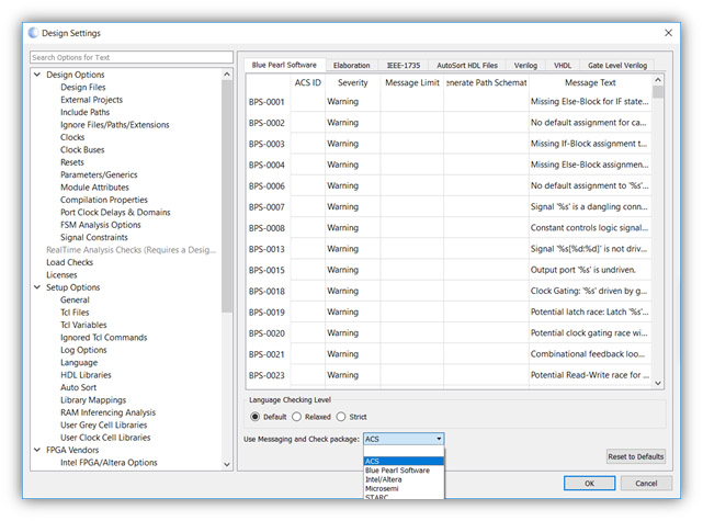
You will notice that there are no extra warnings associated with the Adiuvo Package. This is because we have not yet enabled the messaging and check package. We can do this in the Design Settings à Messaging page, from the drop-down tab select the ACS package which is the name of the extra info package we created in the Tcl script. We can also add this into the Tcl script using BPS::set_msg_check_package command.

6_designsettings2

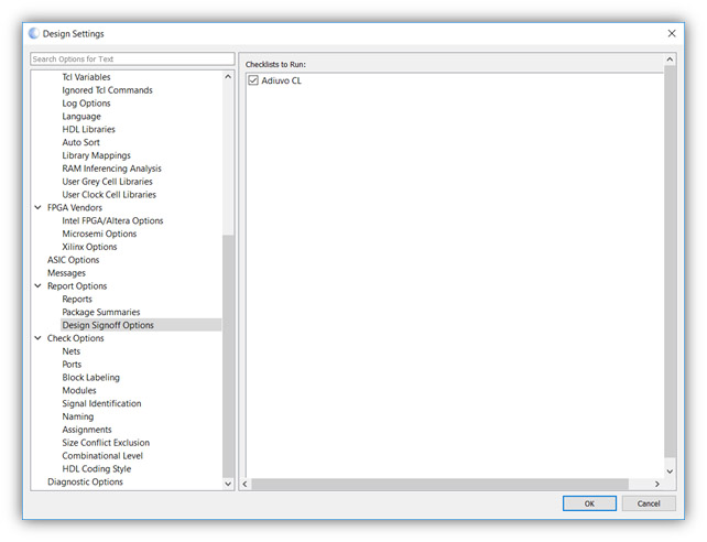
We also need to enable the checklist we previously created. Enabling the checklist will provide a detailed design sign off report along with providing more information for Management Dashboard. This can be achieved via the Design Settings à Report Options à Design Signoff Options page.

7_designsignoffoptions

When we rerun the design analysis again with this message package and check list enabled. In the main window we will see the design sign off report indicating a failure of the SLCC check.

8_designsignoffreport

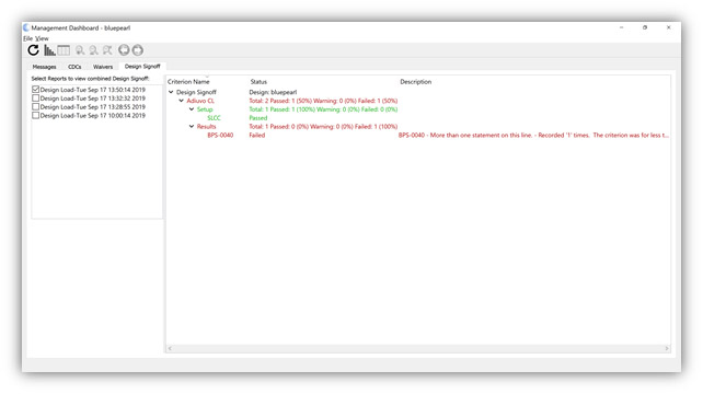
If we open a Management Dashboard, we will see on the Design SignOff tab the Adiuvo checklist was enabled to run and all the checks contained within it were also enabled to run. While the actual results show, an issue was found.

Providing information on both the Design Signoff setup along with the actual results is very important. If a check is reported as having zero issues it can mean either the test found no issues, or the test was not enabled. As such the checklist setup information allows us to demonstrate the test was enabled preventing inadvertent indication that no issues are present.

9_managementdashboard

Investigating further when we open the results view, we will see an additional column in the results with the exact ACS messages from our new package.

10_investigation

Now we know how we can create custom packages of checks which align with our design rules and are reported via custom checklists. We also know how to use the extra message info to add specific information about how the design check relates to our design rules easing any corrective actions.

You can find the example files here https://github.com/ATaylorCEngFIET/BluePearl_VVS

Issue 3: Working with Xilinx Parameterized Macros for CDC

When it comes to crossing clock domains it is best, if possible, to implement the crossing using registers which are located close together and have small set up and hold windows. In short, our register structures used for clock domain crossing should be optimized for signals which may go metastable.

In our Xilinx designs this means we need to use either the HARD_SYNC primitive, or alternatively if our CDC issues are more complex, one of the Xilinx Parameterized Macros (XPM). Xilinx Parameterized Macros can be used to implement CDC, FIFO and BRAM solutions in your design. When it comes to working with BRAM and FIFO, unlike using the BRAM/FIFO generator which uses black boxes in synthesis, XPMs are not black boxed and therefore enable the synthesis tool to make better timing and resource estimates. They also allow for faster simulation than when using the BRAM/FIFO generator. We can use these libraries in 7 Series, UltraScale and UltraScale+ families.

Of course, we are interested in the seven-clock domain crossing (CDC) capabilities provided by XPM. These are:

  • Single Bit Synchronizer – Synchronizes a single bit vector between clocks.
  • Asynchronous Reset Synchronizer – Synchronizes an asynchronous reset to the destination clock. Reset assertion is asynchronous while the reset removal will always be synchronous and safe for the destination clock.
  • Gray Code Synchronizer – Synchronizes a data bus between source and destination clocks, using Gray coding. Using this implementation, the input can only increment or decrement by one between values, making it useful for counters.
  • Handshake Synchronizer – Synchronizes a data bus between source and destination clocks using handshaking of signals.
  • Pulse Synchronizer – Synchronizes a pulse of any width (one source clock cycle or wider) from the source domain to the destination domain.
  • Single Bit Synchronizer – Synchronizes a single bit from source to destination domain.
  • Synchronous Reset Synchronizer – Synchronizes a synchronous reset to the destination clock domain. This both asserts and de-asserts the reset synchronously, unlike the Asynchronous reset macro.

Let’s look at how we can create a simple example using XPM CDC functions and verify the crossings as safe using Blue Pearl Software’s Visual Verification™ Suite.

The code itself for this demonstration is quite simple and will contain two clock domains. The first clock domain will contain a simple counter which counts to a terminal value. This counter can be restarted by a restart signal and reset asynchronously.

Both the restart signal and asynchronous reset are contained within the second clock domain and as such require crossing from one clock domain to another. To perform the clock domain crossing I used the Single Bit Synchronizer and Asynchronous Reset Synchronizer.

Using the Xilinx Vivado™ Design Suite to simulate the design (available on my GitHub), you can see the asynchronous reset and start signals being retimed by the XPM CDC Macros.

layout-design1

When we load this design into the Blue Pearl Visual Verification Suite we can confirm that we have correctly and safely crossed the clock domain.

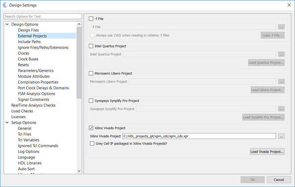
The first thing we need to do in VVS is the import the Vivado project. We can do this using design settings and selecting the external projects dialog and pointing VVS to our Vivado project.

layout-design2

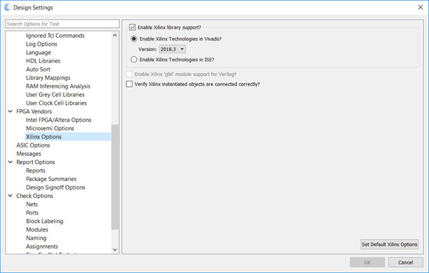
We also need to select the version of the tool we are using on the FPGA Vendors dialog

layout-design3

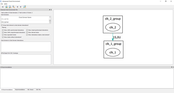
Once that is complete, we can load the design. However, before we run the full CDC analysis, we may want to explore the Advanced Clock Environment which shows relationships between clocks and gives a preliminary indication of whether signals are synchronized or not. In this case we should see we have one signal which is passing from clock domain two to one and is synchronized.

layout-design4

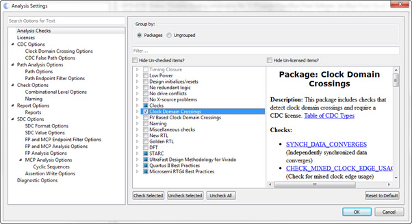
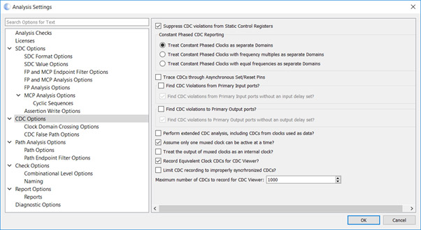
To ensure the clock domain crossings are correct we run the CDC analysis. To do this we need to first ensure that the CDC analysis checks are enabled in the analysis settings.

layout-design5

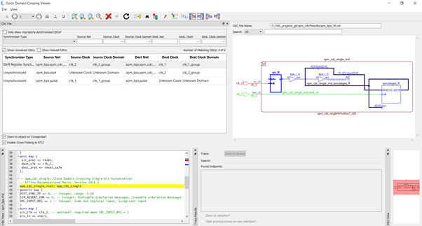
Running this analysis and then opening the Clock Domain Crossing Viewer will show three crossings. If you only see two, ensure the “only show improperly synchronizes CDCs?” check box is NOT checked.

You will then be able to see three crossings, the first a correctly implemented crossing from clock domain two to one. Cross probing to the source code will highlight the XPM instance.

The remaining two are associated with the input and output signals as the clock is not defined for those signals.

layout-design6

There are two ways we can address this issue. We can use an SDC file to associate the inputs with a clock domain. Alternatively, we can uncheck the “Find CDC Violation on Primary Input/Output ports” check box option.

layout-design7

When we rerun the analysis now, we will see only one properly synchronized crossing from clock two to clock one.

Now we understand how we can use XPM CDC structures to perform safe clock domain crossings in our Xilinx devices and that VVS will pick up and identify XPM CDC structures correctly. This enables us to focus on clock domain crossings which might have been missed in the VVS CDC environment.

You can obtain the Vivado project and design files here if you wish to experiment with XPM and VVS.

To read more about the Xilinx / Blue Pearl integration in our white paper.

Issue 2: Identifying & correcting difficult to find RTL problems earlier

All engineers know the earlier we identify an issue in our design, the easier and less costly it is to correct. We also know some issues are easier than others to identify. The worst kind are those which are intermittent and manifest late in the test regime or, even worse, in the field. These late arising issues lead to many long hours and stress in the engineering team as we try to address the root cause.

While these root causes may be varied, we can group them together into several likely classes which may be the root cause. These include:

  • Missing Assignments – Missing assignments arise from how we write the code, for example an IF check not having a corresponding ELSE or missing a CASE statement. Structures such as this will result in different behaviour depending on the synthesis tool, inferring either latches or registers. The latch will of course behave differently which impacts portability and may result in issues in corner cases, which are hard to track down.

issue2_1

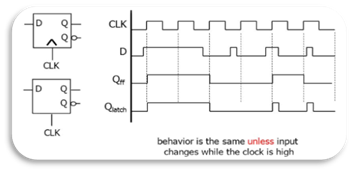
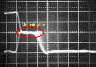
  • Clocking – Modern designs contain several clock domains. Of course, information needs to be shared between these domains. Incorrect synchronisation of data and signals between clock domains can result in metastability and corrupted data. In some systems this incorrect data can be catastrophic. Most engineers will use two stage synchronisers and FIFOs to transfer data safely however, due to the complexity of designs, signals can slip through the net and be unsynchronised. One example which can be hard to find is using a FIFO status signal e.g. Full or Empty on the wrong clock domain. This will lead to intermittent behaviour which might not be found until late in the product life cycle.

issue2_2

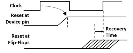
  • Reset – Incorrect handling of asynchronous reset release or de-assertion can lead to metastable events if reset release changes during the flip flop’s hold or set up time. As the relationship between the reset and clock is asynchronous, this relationship will change each time the board is powered. We also need to consider the internal routing delays of the reset signal; what may look good at the pins is still an issue at the flop as delays in routing can also introduce metastability.

issue2_3

  • Finite State Machine (FSM) Behaviour – FSM are the heart of our designs; they are how we implement sequential control structures in our FPGA and ASICs. The more complex the FSM, the harder it is to visualise and ensure all states are reachable and that a transition to a state is not terminal. If state machines have inadvertent terminal states, the state machine will lock up and be unrecoverable unless power cycled or reset.

issue2_4

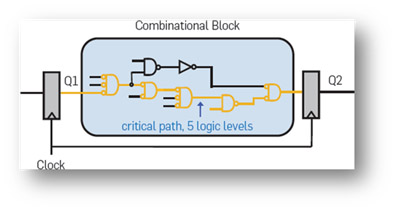
  • Longest Path – Long combinatorial paths between registers impacts the maximum frequency with which we can achieve timing closure. This can also cause issues during the place and route when paths which fail timing are incorrectly reported as being the longest path (In reality they are the longest paths failing timing).

issue2_5

When we generate our designs, we are of course aware of these issues and attempt to mitigate these using independent code reviews and coding standards. However, as designs get larger and more complex it is hard to detect and verify them all.

This is where tools such as Blue Pearl Software’s Visual Verification Suite comes into their own. Let’s take a quick look at how we can use the suite of tools to identify and address these issues.

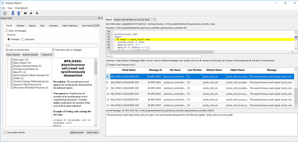
When we load a design into the suite, the design is subject to several (configurable) load checks, which check for missing assignments and reset behaviour along with several other checks. These load checks enable us to identify issues such as asynchronous reset synchronisation, missing assignments and undriven logic.

issue2_6

To ensure our FSMs behave as expected, we can use the FSM viewer to visually verify the behaviour of the state machine. This is to ensure that each state has entry and exit points and that no state becomes a terminal state from which once entered there is no exit.

issue2_7

Of course, at the heart of suite is the Clock Domain Clocking (CDC) analysis capability, which enables us to identify Clock Domain Crossings which are not correctly synchronised. Once identified we can quickly and easily implement a solution which addresses the identified issue. As in the example below where the empty flag is used in conjunction with the write clock without synchronisation, this will at times result in a very hard to find intermittent metastability issue.

issue2_8

Now we have outlined some of the key design challenges which can impact our design late in the development cycle or even worse in the field and how we can identify and correct these. Over the next few blogs we are going to take a deeper look at how we can use the suite to identify and correct these issues.

If, however, you cannot wait, why not join me at DAC 2019 in Las Vegas where I am running a lunch and learn on Monday at the Blue Pearl Software booth #345.  I will be demonstrating how we can use Visual Verification Suite to find and correct these design issues and more.

Getting Started with Blue Pearl Issue One: Introduction

Our FPGA and SoC designs are increasingly complex and used for a wide range of applications from autonomous driving to image processing, machine learning, defence, aerospace and space applications.

Of course, while complexity has increased the available development time has been static or reduced. Indeed, both the AspenCore embedded survey 2017 and 2019 indicate the two largest challenges in delivering a project are meeting schedule and debugging the application[1].

When it comes to developing our FPGA and SoC based solutions, just like in any engineering endeavour the earlier we can identify issues the easier, timelier and less costly they are to address.

Early identification of issues within our FPGA or SoC design is where Blue Pearl Software comes into its own. If this is the first time you have come across Blue Pearl, their suite of verification tools enables us to Visualize the design, Verify the structure and Validate the design.

In this series of blogs, we are going to explore how we can use Blue Pearl’s Visual Verification Suite™ and leverage its capabilities to assist in our FPGA/SoC designs.

In this first blog we are going to start at the very beginning and look at what design visualisation features = the suite offers to use as FPGA/SoC Designers.

Blue Pearl’s visualisation of the design enables us to perform the following:

  • Analyze RTL™ linting and debug – This enables us to ensure coding standards are followed, analyse the design for several structural issues, verify the design complies with manufacturer coding standards e.g. Xilinx Ultrafast Methodology, run path analysis and explore finite state machines.
  • Clock Domain Crossing – Analyse design and clocking structures to ensure CDC is implemented correctly in the design.
  • Automated SDC generation – Identified false paths and multi-cycle paths in your design and generated the appropriate SDC file.

To provide visibility of the results of the analysis and verification checks the Management Dashboard is provided.

In the remainder of this blog we are going to look at where in the development cycle we should use the Blue Pearl suite, and how we can get started with our first design.

As I mentioned previously, the earlier we can identify issues the easier and less costly they are to address. As such we should be using Blue Pearl throughout the development of the HDL prior to starting simulation.

Of course, the following stages of development simulation, synthesis and place and route can result in RTL changes. If there are RTL changes, we should re run the Analyze RTL to ensure no issues have been introduced.

https://m.eet.com/media/1246048/2017-embedded-market-study.pdf

bps_1

Once we have the Visual Verification Suite  Installed (you can get a evaluation copy here) the next step is to open the suite and then open the getting stated design example.

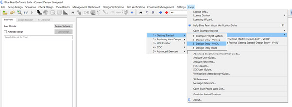
To open the getting started example we should select Help->Open Example Project -> Getting Started and then select your preferred language VHDL or Verilog.  As I am a VHDL user I will open the VHDL design entry example.

bps_2

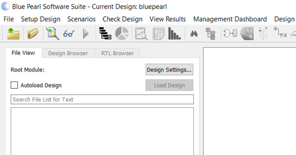
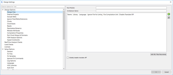
To load in the design files, we need to select the Design Settings button

bps_3

To actually add RTL files, we need to click on the green add file option under the Design Files option

bps_4

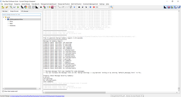
Once all the source files are added, click on OK and the click on load design back on the suites start page. After a few second you will see the design has loaded and that there are no errors but some warnings.

bps_5

With the design loaded we can start examining the RTL design analysis. The first step of which is to open the Real Time Analysis and Dependency viewer.

We can open the Real Time Analysis viewer by clicking on the highlighted button below.

bps_6

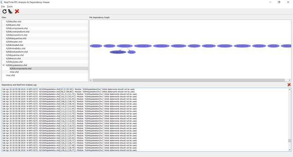
This will open the Real Time Analysis and Dependency viewer. The dependency viewer does not outline the hierarchy instead it outlines how the files are interrelated.

bps_7

Understanding this interrelationship is very useful when we come across issues during design loading.

Now we have our design loaded we are ready to start exploring our design space using the suites analysis and design checking options.

We will start looking at these in the next blog soon!

Improving the quality of spacecraft RTL using HDL linting

If you have ever aspired to write out-of-this-world RTL, there’s never been a better time as satellites, spacecraft, landers, and rovers are increasingly using FPGAs and ASICs in their sub-systems.

Some recent peer-reviews have highlighted poor coding techniques that have resulted in space-electronics failures, e.g. a $1M CubeSat becoming inoperable by getting trapped in a finite state machine’s dead state. HDL linting, including structural static analysis, can check the quality of RTL before simulation, synthesis, and implementation, and has proven to be so effective in identifying bad practices for high-reliability applications that some satellite manufacturers now mandate their HDL programmers lint files before they are formally checked-in. The run time is significantly shorter than logic simulation and it can be performed early in the design cycle, where mistakes are less expensive, and while RTL is being developed, without requiring an exhaustive testbench.

Linting parses RTL identifying issues such as race conditions, register conflicts, bus contention, implied latches, redundant logic, X-propagation, long paths, and dead states. The analyses allows company-specific standards to be set up to enforce coding clarity and naming conventions.

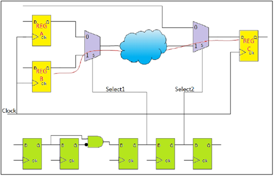
Structural static analysis can find false paths directly from the RTL where no sequence of inputs results in an event propagating along the path and can thus be ignored for timing analysis and optimising performance. For example, the path from Register B to C shown below can never be sensitised because the output from the cloud of logic is de-selected at MUX2.

Figure 1 Example of single-cycle false path

Some false paths require multiple cycle across many levels of hierarchy to complete their function such as pulse generators or pipelined structures. For example, Select1 and Select2 shown below cannot be high at the same time resulting in a false path.

multi_cycle_false_path_example

Figure 2 Example of multi-cycle false path

Structural static analysis can find the longest path critical to achieving timing closure and device fit: identifying false and multi-cycle paths directly from the RTL helps synthesis and implementation avoid unnecessary effort to meet timing or other optimisations on those nets. Needlessly placing and routing false paths can cause critical logic to miss closure!

Linting improves the quality of reliability (QoR) of RTL by identifying poor coding early in the development cycle when engineers are under less pressure to finish. It reduces design risk, accelerates IP verification, increases productivity, and reduces debugging effort and test time spent in the lab to meet time-to-market deadlines.

An example of linting and structural static analysis increasingly being adopted by the space industry to improve the quality of RTL and sign-off IP is Blue Pearl’s Visual Verification Suite. By using this software, Orbital ATK working on a NASA project recently detected 24 clock-domain crossing (CDC) errors in production SpaceWire IP that were not picked up by traditional formal-verification methods.

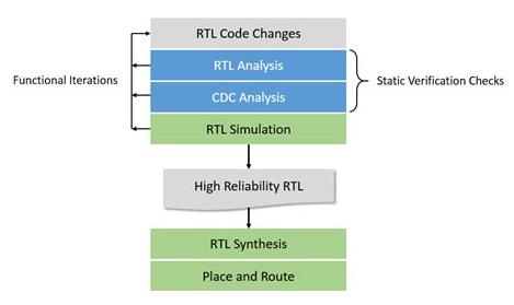
The Visual Verification Suite parses RTL before simulation and synthesis checking for quality and reliability problems followed by CDC investigations. Code is analysed in a sequence where the first issues addressed are either those whose solution will also fix other faults or may cause or reveal other types of problems that can then be examined separately. The diagram below illustrates where HDL linting and structural static analysis fits within the standard FPGA/ASIC design flow.

figure3

Figure 3 Blue Pearl’s HDL linting flow

Spacechips peer-reviews space electronics and RTL for many satellite and spacecraft manufacturers and we have started evaluating Blue Pearl’s Visual Verification Suite to check the quality of third-party IP. Given that we do not always know the original design intent, HDL linting has proven to be useful in debugging and verifying the functionality of code. A very useful feature of the software is its ability to automatically detect and quickly validate the behaviour of finite state machines using bubble diagrams to display all states and transitions between them, as well as identifying unreachable ones. Previously, we would have written exhaustive test benches, which is time consuming.

The software also analyses CASE statements reporting duplicate, overlapping, or missing items, as well as absent assignments or the default clause. The linter can be extended, allowing custom checks to be created using Tcl or SDC (timing constraint) commands. During linting and structural static analysis, the tool can be controlled using its interactive GUI or run automatically in batch mode using Tcl.

As digital space electronics complexities increase, avionics engineers are increasingly using commercial or existing IPs to meet time-to-market deadlines. Typically, these come in various formats, (e.g. synthesizable RTL, encrypted IP, simulation models, or non-synthesizable HDL), often from disparate sources, and operate with independent clocks with different frequency and phase relationships, i.e. separate domains.

With multiple domains containing non-integer-related or drifting clocks, one has to verify the synchronicity of signals going between them. CDC occurs when data is transferred from a flip-flop driven by one clock to another triggered by a different clock. Setup and hold violations can result in metastability, which can propagate through a design as an erroneous state causing functional failure. Traditional simulation and static-timing analysis cannot model this behaviour and are unable to confirm if data is transferred consistently and dependably across domains.

If third-party IP is delivered as synthesizable RTL, then CDC analysis can be performed on these. However, for other formats, instantiated blocks have traditionally been imported as black boxes, containing sensitive, proprietary IP, and the analysis has been unable to use any knowledge of their internals nor information regarding the interaction of ports with clocks.

The Visual Verification Suite supports the concept of a grey cell that provides clocking and register information for third-party IP, allowing for accurate CDC analysis beyond what is possible using the traditional black-box methodology. A grey cell is a representation of a module that excludes all internal register-to-register logic, including only all logic from each input up to and including the first register, and all logic from each output back to and including the last register. Grey cells preserve the confidentiality of third-party IP as shown below.

black_box_ip_vs_grey_cell_ip

Figure 4 Black-box IP vs. grey-cell IP

For users of space-grade FPGAs, Blue Pearl’s Visual Verification Suite is supported by Microsemi’s Libero SoC and Xilinx Vivado IDEs. To help the space industry manage increasingly complex designs instantiating IPs from many different sources, e.g. FPGA/ASIC providers, space agencies, OEMs and third-parties, I recommend that all providers of high-reliability FPGAs and ASICs include linting and structural static analysis within their design environments to allow HDL programmers to improve the quality of RTL.

HDL linting, including structural static analysis, improves the quality of spacecraft RTL and reduces risk earlier in the design cycle, allowing IP to be signed-off with confidence. I intend to continue the discussion by presenting a webinar sharing examples of poor coding and demonstrating how Blue Pearl’s Visual Verification Suite improves QoR of RTL, accelerates IP verification, decreases development time, and increases productivity to help meet time-to-market deadlines.

Adam Taylor’s MicroZed Chronicles, Part 227: Blue Pearl Visual Verification Suite automates design checking to improve design quality

Over the last couple of weeks, we have examined how we can debug our designs using Micrium’s μC/Probe (Post 1 and Post 2) or with the JTAG to AXI Bridge. However, the best way to minimize time spent debugging is to generate high quality designs in the first place. We can then focus on ensuring that the design functionality is as specified instead of hunting bugs.

To improve the quality of our design, there are several things we can do that help us achieve timing closure and identify design issues and bugs:

  • Review code to ensure that it not only complies with coding and design standards and to catch functional issues earlier in the design stage.
  • Ensure compliance with device/tool-chain-recommended coding standards—for example the Xilinx Ultrafast design methodology.
  • Correctly constrain the design for clocks, multicycle, and false paths.
  • Analyze CDCs (Clock Domain Crossings) to ensure that all CDCs are correctly handled.
  • Perform detailed simulation to test corner cases and boundary conditions.

Over my career, I have spent many hours performing code reviews, checking designs for functionality, and for compliance with coding standards and tool-chain recommendations.

The Blue Pearl Visual Verification Suite is an EDA tool that automates design checking over a range of different customizable rule sets including basic rules, Xilinx Ultrafast design methodology rules, and DO254. The Blue Pearl tools also perform detailed analysis of clocks, counters, state machines, CDCs, paths, and constraints. All of this checking helps engineers gain a better understanding of the functional side of their design. In short, this is a very useful tool set to have in our tool box to improve design quality. Let’s look at how this tool integrates with the Xilinx Vivado design environment and how we can use it on a simple design.

With Blue Pearl installed, the first step is to integrate it with Vivado. To do this we use the Xilinx TCL Store to install the Blue Pearl Visual Verification Suite.

xilinx1

Installing Blue Pearl via the Xilinx TCL Store

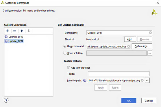
Once Blue Pearl is installed, the next step is to create two custom commands. The first command allows us to open a new Blue Pearl project from an open Vivado project. The second command allows updates from Vivado into the Blue Pearl project.

We create these custom commands by selecting tools->custom commands->customizes commands.

bps_tools_report

Open the Command Customization dialog

This opens a dialog that allows you to create custom commands. For each command, we need to define the callable TCL procedures in the Blue Pearl Visual Verification Suite.

bps_cmds

Creating the Launch BPS command

For the “launch BPS” command, we need to use the command:

::tclapp::bluepearl::bpsvvs::launch_bps

Creating the Update Command

Creating the Update Command

For the update BPS command, we call the following command:

::tclapp::bluepearl::bpsvvs::update_vivado_into_bps

Once you have completed the addition of the customized commands, you will see two new buttons on the Vivado tool bar.

With the integration completed, we can now use Blue Pearl to analyze and improve the quality of our design if we identify issues that need analysis. Clicking the newly created “launch Blue Pearl” command within a Vivado project opens a new Blue Pearl project for analysis.

As it loads the Vivado design, Blue Pearl checks the code for synthesis and identifies any black boxes. Any syntax errors encountered will be flagged for correction before further analysis can be performed.

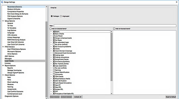
There are an extensive number of checks and analysis that can be run on the loaded design, ranging from basic checks to DO254 compliance. There are so many possible checklist items that it might take a little time to select the checks that are important to you. However, once you’ve specified the checks you want, you can save the rules and use them across multiple projects. What is interesting is the tool also reports if the check has been run and not just its status as pass of fail. This explicit feedback mechanism removes the ability of designers to achieve compliance by omission. (And that’s a good thing.)

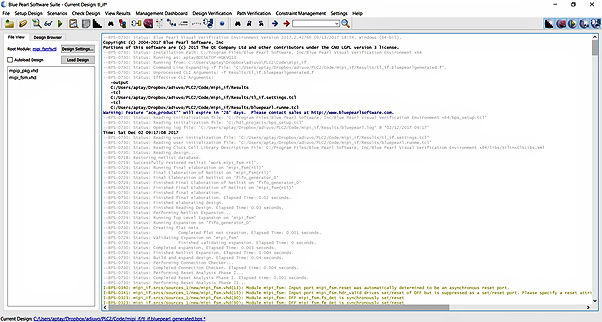
Blue Pearl Environment

Blue Pearl Environment

Design Check configuration

Design Check configuration

As an example, I loaded a project that I am working on to see what the design check and analysis reports look like. The design is simple. It decodes a MIPI stream to frame sync, line sync, and pixel values. While this is a simple design, Blue Pearl still identified a few issues within the code that need consideration to see if they present an issue or not.

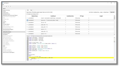
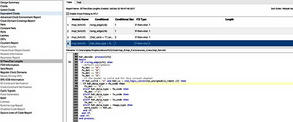
The first potential issue identified was in the If/Then/Else (ITE) analysis. The design contains a VHDL process that decodes the MIPI header type. This process is written using an if / elsif structure, which implies a priority encoder. Furthermore, to differentiate between five different header commands, the length of the priority encoder contains a five deep if / elsif structure. Blue Pearl calls this a length of five. By default, Blue Pearl generates warnings on lengths greater than 3. In this case no priority required and a case statement would provide better synthesis results because there is no need to consider input priority. Although each application is different, you as the engineer need to use your own experience and knowledge of the design to decide whether or not priority is needed.

Along with reporting the length of the if structure, ITE analysis also analyzes the number of conditions within a statement. This is important when an if statement contains several conditions because additional conditions require additional logic resources and routing, which will impact our timing performance.

identification

Identification of if / then /else large length

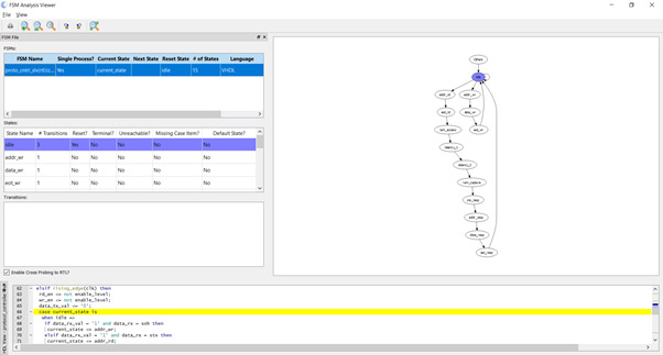
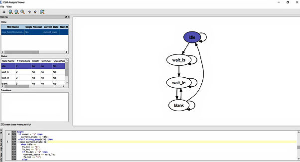
State machines are of course used in designs for control structures. Complex control structures requires large state machines, which can be difficult to follow in the RTL. As part of its analysis, Blue Pearl creates visualizations of state machines within a design. This visualization details the transitions among states, along with identifying any unreachable states. I found this capability very useful not only in debugging and verifying the behavior of my own state machines, but also for visualizing third-party designs. This graphical capability definitely helps me understand the designer’s intent.

FSM Analysis Viewer

FSM Analysis Viewer

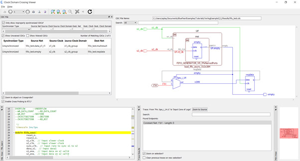
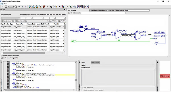
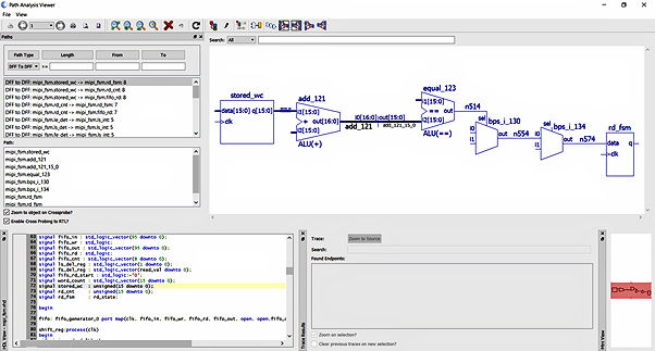
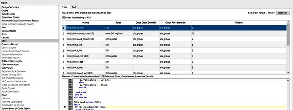
Blue Pearl also provides the ability to visualise CDCs and paths and to monitor fan out within a design. These features allow us to identify places in the design where we might want to add CDC-mitigation measures such as re-timing or pipeline registers within the design.

Clock Domain Crossing Analysis

Clock Domain Crossing Analysis

Path Analysis

Path Analysis

Flip-Flop Fan out reporting

Flip-Flop Fan out reporting

Having touched lightly on the capabilities of Blue Pearl, I am impressed with the results once you have taken the time to set the correct checks and analysis. The analysis provided allows you to catch potential issues earlier in the design cycle, which should reduce the time spent in the lab hunting bugs. In turn, this frees us to spend more of our time testing functionality.

You can find the example source code on GitHub.

Adam Taylor’s Web site is http://adiuvoengineering.com/.

If you want E book or hardback versions of previous MicroZed chronicle blogs, you can get them below.

First Year E Book here

First Year Hardback here.

Adam First Year Book

Second Year E Book here

Second Year Hardback here

Adam Second Year Book

The Value of High Reliability RTL for FPGA Design

Introduction

high_reliability_rtl Today’s FPGA designs are typically developed by assembling between 50 to 100 unique IP blocks to form a complete System on Chip (SoC) including embedded processors, high speed serial interfaces, analog, signal processing and control logic. These systems are large, complex and partitioned into multiple clock domains and reset structures required to interface and control the various subsystem and reduce overall system level power. FPGA designers, developing these advance SoCs, must not only develop functionally correct RTL, they must also meet conditions for downstream interoperability within the overall system.

To reduce design risk and schedule slips, RTL code must be free of design errors, adhere to industry and corporate best practices, be free of dead code and unreachable finite state machine (FSM) states, in addition to having synchronized clock domains crossings to ensure metastability. Failure to use high reliability RTL can result in difficult and time consuming system level debug as well as design iterations late in the design process when iteration times are at their longest.

High reliability RTL is best achieved through a structured development environment that incorporates design automation for static design verification. While FPGA vendor supplied synthesis and place and route tools do identify many design rule violations, more sophisticated checks are needed earlier in the design processes. Two separate analysis environments are required; RTL Analysis for for bus contention, register conflicts, race conditions and CDC (clock domain crossing) analysis to identify asynchronous clock domains and their crossings.

agile_design_flow

Without automation, finding and remedying design errors that affect interoperability turns into a random manual exercise. Automation enables an agile design process where developers continuously identify and address design errors while writing the RTL making it easier to develop, easier to test, and more reusable for future designs.

Blue Pearl Software

Blue Pearl Software, Inc. is a provider of design automation software for ASIC, FPGA and IP RTL verification. Its Analyze RTL™ linting and debug, Clock Domain Crossing analysis and Synopsys Design Constraints (SDC) generation solutions are proven to improve quality-of-results (QoR), reduce risk and decrease development time. The Visual Verification Environment complements RTL simulation solutions provided by EDA and FPGA vendors by ensuring code and SDC quality along with clocking integrity. Engineered to maximize RTL find/fix rates, the Visual Verification Suite uniquely provides easy setup, consistent results, Management Dashboard for complete push-button analytics, and runs on both Linux and Windows.
RTL Analysis with Lint Checking, Formal Verification and X-Propagation

Analyze RTL incorporates a suite of technologies into a single RTL analysis environment to help developers find bugs earlier in the design processes. Super-lint tools are combined with the power of formal verification to provide a single, high capacity design checking environment that identifies poor coding styles, improper clocks, simulation and synthesis problems, poor testability and other source code issues. FSM analysis automatically extracts and analyzes finite state machines for dead or terminal states and provides a visual representation. X-propagation analysis will detect unknown states, often introduced into designs to implement soft resets or to implement power management schemes that are masked during RTL simulation.
Clock Domain Crossing Analysis with Grey Cell Technology

Blue Pearl delivers the industries most advanced clock domain crossing analysis that incorporates over a decade of experience to find errors other tools fail to identify. Analyzing RTL for a single block of a system in isolation is not sufficient to detect all CDC violations but rather the entire system must be considered and analyzed to perform a thorough CDC analysis. However, this can be a challenge when using 3rd party encrypted IP. Blue Pearl addresses this challenge using a patented technology called “Grey Cell” that enables a representation of a protected IP block for CDC analysis of module-to-module connections while preserving the trade secrets of the original IP provider.

system_modeling_using_grey_cell

Architected for Ease of Use Ensures Fastest Bug Find/Fix Rate.

Even the best static verification technology can be severely hampered by poor usability as potentially thousands of errors may be detected and flagged to the user for resolution. The Visual Verification Environment addresses the static verification usability problem in three key ways. First it includes a graphical user interface that incorporates state of the art EDA “ease-of-use” concepts that is proven to make new users productive in under 2 days. Tool options and settings are progressively displayed to the user with quick links to documentation. Second, a powerful set of message filters have been developed that lets users quickly identify only those messages that need attention. Design teams can focus on issues requiring direct attention and not be distracted by items of limited or no importance. And third, the environment provides a schematic view of the RTL with cross probing back to the warning or error message and RTL source code that lets users quickly understand and resolve each message that requires attention.
Industries only Static Verification Tool Optimized for FPGAs

Blue Pearl offers the only static verification environment optimized for the unique requirements of FPGA design. These checks include analyze for routing congestion, reset configurations and even estimate critical timing paths prior to synthesis. Grey Cell modeling supports the analysis of FPGA vendor provided protected IP cores with asynchronous clock domains. The Visual Verification Suite supports both Xilinx Vivado® Design Suite with built in UltraFast™ Design Methodology design rules and Altera’s Quartus® Prime Design Software and is the only static verification environment that runs on Windows – the preferred FPGA environment.

Summary

The Blue Pearl Visual Verification Suite enables developers to turn functionally correct RTL into high reliability RTL that supports interoperability into IP based system designs. Over a decade of experience is incorporated into industry leading technology that is uniquely optimized for the ease of use with the fastest bug find / fix rate and provides design rules checks required for FPGA design. For more information, please visit www.bluepearlsoftware.com to download an evaluation today.

Tcl scripts and managing messages in ASIC & FPGA debug

Our previous Blue Pearl post looked at the breadth of contextual visualization capability in the GUI to speed up debug. Two other important aspects of the ASIC & FPGA pre-synthesis workflow are automating analysis with scripts and managing the stream of messages produced. Let’s look at these aspects in the latest Blue Pearl 2016.1 release.

An important aspect to regression testing is to run exactly the same tests as a design is iterated. The solution is scripting, automating the types and sequence of analysis with a saved file for execution. Tcl is a powerful scripting language popular in EDA circles, and rather than stay with their own syntax Blue Pearl has chosen to migrate their tools entirely onto Tcl. However, instead of providing only a command line interface usually associated with Tcl, they’ve taken the idea farther.

Blue Pearl Tcl integration

Both the GUI and the CLI are Tcl-based in the new release of the Blue Pearl suite. Set up can be done in the GUI and it can launch tests in the Core Analysis engine. For more complete test runs typically performed overnight, a Tcl script can be created and kicked off in the command line. Upon returning the next day, the CLI run can be loaded back into the GUI to allow the full visualization capability we discussed in our previous installment. This level of integration allows customized scripts for control, comparison of results from current and past runs, and rapid debug.

Those results are fundamentally a list of messages. With a well-designed message syntax, regular expressions can be used to process the list. In a sizable design with a long list of analysis messages, users will typically want to filter the list by different criteria. The Blue Pearl GUI allows some quick filtering capability via check boxes. More powerful message waiver capability now exists, including wild carding and string matching, which can be applied to a result set or removed – the results themselves are unmodified, only the managed view with waivers applied. This is handy where there are stylistic differences in code reviews; what one team considers a warning may be a mandatory fix for another.

Messages can also be customized and grouped. Since the messages are stored in a SQL database – as are many other EDA tool messages – scripts can read text from other sources such as synthesis tools and add those messages into the Blue Pearl database. (Note in the image below the Xilinx Vivado messages have been incorporated.) The GUI can then sort, filter, waive, and compare messages accordingly. When developing with unique internal coding standards, this user-extendable capability is essential to ensuring consistency and efficiency.

Blue Pearl message grouping

Our focus in these Blue Pearl posts has been on usability of the tools rather than specifics of results in RTL and CDC analysis. The pre-synthesis checks Blue Pearl performs are extensive. Designers adopting these kinds of tools are generally not looking for something that generates a huge list of issues to sort through – they are looking for actionable items. The real need is tool that brings attention to the most urgent issues, and allows less interesting results to be kept in the background.

The idea behind “continuous integration” of chip designs is to provide a gate, a quality check difficult to implement with manual methods. The twist is that gate is not cleared once, but has to be cleared every time the design goes back for synthesis with any change. A process leveraging the Blue Pearl suite delivers more predictability in designs with automated checking and efficient debug.

Great news for ASIC & FPGA designers in their daily tasks, but what about that dreaded project review when engineers have to show management what is happening with the schedule? Next, we’ll explore what Blue Pearl is doing in the area of metrics, leading up to their big announcement at DAC in Austin.